You are here:
Home » Products – Immersion tin
Immersion tin process
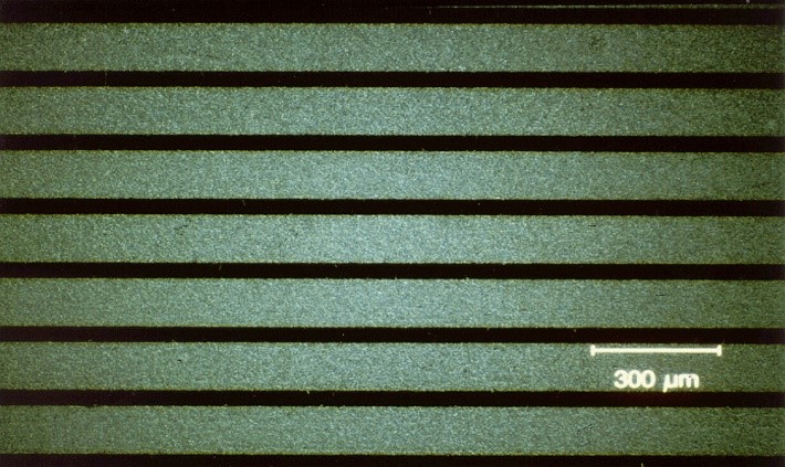
Fine-Line application – Conductor spacing 50µm.
BECE STANOSIT-EC 2002 – Precise and reliable tin deposition as final surface.
The BECE STANOSIT-EC 2002 process is a powerful immersion tin plating system specifically designed to meet the demands of modern PCB manufacturing. With its high reliability and user-friendly operation, it provides an optimal solution for immersion tin deposition on copper surfaces.
Outstanding Features
- Uniform Tin Layers: Produces flat, fine-grained, and dense tin layers on even the smallest copper surfaces, with a layer thickness of 0.8–1.2 µm and excellent solderability-compatible with Pb-free and Sn/Pb solders.
- Bridge Prevention: Immersion tin deposition effectively minimizes the risk of tin bridges between individual pads, reliably preventing short circuits.
- Gentle Processing: The low process temperature of only 70 °C reduces thermal stress and protects the PCBs.
Efficient Process Management
- Predip Solution: BECE STANOSIT-EC 2002 Predip prevents contamination of the main tin bath and enhances deposition and surface results through light pre-tinning at room temperature.
- Easy Operation: Ready-to-use solutions and a single replenisher for both the predip and the main tin bath make process control quick and straightforward.
- Extended Bath Life: Special additives minimize tin-IV formation, increasing the process stability and efficiency.
Copper Control for Optimal Results
- During tin deposition, approximately 1.1 g of copper dissolves for every 1.0 g of tin deposited.
- When the copper concentration reaches 7 g/l, the tin layer properties may be affected.
- Copper can be efficiently removed as a complex by cooling to room temperature, extending the bath life.
Versatile Application
The BECE STANOSIT-EC 2002 process is suitable for use in both vertical dip systems and horizontal flow systems, making it a versatile solution for immersion tin deposition.
KEY PRODUCT ADVANTAGES
Properties of the tin layer:
- Flat, uniformly thick, and fine-crystalline layer
- Layer thickness depending on immersion time: 0.3 - 1.2 µm
- No tin bridges, meaning no short circuits
- Solderable even after "aging" for 4 hours at 155 °C
- High surface resistance of the coated PCB
- Suitable for press-fit technology.
- Ideal for fine-pitch SMD technology
Properties of the tin layers:
- Simple process management
- Copper absorption up to 7 g/l possible without quality loss
- Extension of bath life possible through copper depletion
- Suitable for immersion processes (vertical) and conveyor processes (horizontal)
Before and After Visualization:
